- 您现在的位置:买卖IC网 > Sheet目录446 > IRFR9020TRLPBF (Vishay Siliconix)MOSFET P-CH 50V 9.9A DPAK
�� �
�
�IRFR9020,� IRFU9020,� SiHFR9020,� SiHFU9020�
�www.vishay.com�
�THERMAL� RESISTANCE� RATINGS�
�Vishay� Siliconix�
�PARAMETER�
�Maximum� Junction-to-Ambient�
�Case-to-Sink�
�Maximum� Junction-to-Case� (Drain)�
�SYMBOL�
�R� thJA�
�R� thCS�
�R� thJC�
�MIN.�
�-�
�-�
�-�
�TYP.�
�-�
�1.7�
�-�
�MAX.�
�110�
�-�
�3.0�
�UNIT�
�°C/W�
�SPECIFICATIONS� (T� J� =� 25� °C,� unless� otherwise� noted)�
�PARAMETER�
�SYMBOL�
�TEST� CONDITIONS�
�MIN.�
�TYP.�
�MAX.�
�UNIT�
�Static�
�Drain-Source� Breakdown� Voltage�
�Gate-Source� Threshold� Voltage�
�Gate-Source� Leakage�
�Zero� Gate� Voltage� Drain� Current�
�V� DS�
�V� GS(th)�
�I� GSS�
�I� DSS�
�V� GS� =� 0� V,� I� D� =� -� 250� μA�
�V� DS� =� V� GS� ,� I� D� =� -� 250� μA�
�V� GS� =� ±� 20� V�
�V� DS� =� max.� rating,� V� GS� =� 0� V�
�V� DS� =� 0.8� x� max.� rating,� V� GS� =� 0� V,� T� J� =� 125� °C�
�-� 50�
�-� 2.0�
�-�
�-�
�-�
�-�
�-�
�-�
�-�
�-�
�-�
�-� 4.0�
�±� 500�
�250�
�1000�
�V�
�V�
�nA�
�μA�
�Drain-Source� On-State� Resistance�
�R� DS(on)�
�V� GS� =� -� 10� V�
�I� D� =� 5.7� A� b�
�-�
�0.20�
�0.28�
�?�
�Forward� Transconductance�
�g� fs�
�V� DS� ?� -� 50� V,� I� DS� =� -� 5.7� A�
�2.3�
�3.5�
�-�
�S�
�Dynamic�
�Input� Capacitance�
�C� iss�
�V� GS� =� 0� V,�
�-�
�490�
�-�
�Output� Capacitance�
�Reverse� Transfer� Capacitance�
�Total� Gate� Charge�
�C� oss�
�C� rss�
�Q� g�
�V� DS� =� -� 25� V,�
�f� =� 1.0� MHz,� see� fig.� 9�
�I� D� =� -� 9.7� A,� V� DS� =� 0.8� x� max.�
�-�
�-�
�-�
�320�
�70�
�9.4�
�-�
�-�
�14�
�pF�
�Gate-Source� Charge�
�Gate-Drain� Charge�
�Q� gs�
�Q� gd�
�V� GS� =� -� 10� V�
�rating,� see� fig.� 18�
�(Independent� operating�
�temperature)�
�-�
�-�
�4.3�
�4.3�
�6.5�
�6.5�
�nC�
�Turn-On� Delay� Time�
�t� d(on)�
�-�
�8.2�
�12�
�Rise� Time�
�Turn-Off� Delay� Time�
�Fall� Time�
�t� r�
�t� d(off)�
�t� f�
�V� DD� =� -� 25� V,� I� D� =� -� 9.7� A,�
�R� g� =� 18� ?� ,� R� D� =� 2.4� ?� ,� see� fig.� 17�
�(Independent� operating� temperature)�
�-�
�-�
�-�
�57�
�12�
�25�
�66�
�18�
�38�
�ns�
�Internal� Drain� Inductance�
�L� D�
�Between� lead,�
�D�
�-�
�4.5�
�-�
�Internal� Source� Inductance�
�L� S�
�6� mm� (0.25")� from�
�package� and� center� of�
�die� contact.�
�G�
�-�
�7.5�
�-�
�nH�
�S�
�Drain-Source� Body� Diode� Characteristics�
�Continuous� Source-Drain� Diode� Current�
�Pulsed� Diode� Forward� Current� a�
�I� S�
�I� SM�
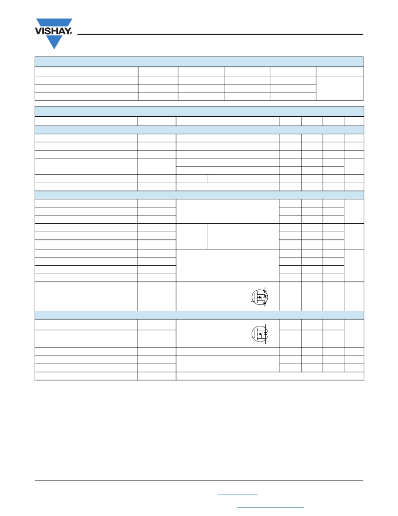
�MOSFET� symbol�
�showing� the�
�integral� reverse�
�p� -� n� junction� diode�
�G�
�D�
�S�
�-�
�-�
�-�
�-�
�-� 9.9�
�-� 40�
�A�
�Body� Diode� Voltage�
�Body� Diode� Reverse� Recovery� Time�
�Body� Diode� Reverse� Recovery� Charge�
�V� SD�
�t� rr�
�Q� rr�
�T� J� =� 25� °C,� I� S� =� -� 9.9� A,� V� GS� =� 0� V� b�
�T� J� =� 25� °C,� I� F� =� -� 9,7� A,� dI/dt� =� 100� A/μs� b�
�-�
�56�
�0.17�
�-�
�110�
�0.34�
�-� 6.3�
�280�
�0.85�
�V�
�ns�
�nC�
�Forward� Turn-On� Time�
�t� on�
�Intrinsic� turn-on� time� is� negligible� (turn-on� is� dominated� by� L� S� and� L� D� )�
�Notes�
�a.� Repetitive� rating;� pulse� width� limited� by� maximum� junction� temperature� (see� fig.� 16).�
�b.� Pulse� width� ?� 300� μs;� duty� cycle� ?� 2� %.�
�S13-0169-Rev.� D,� 04-Feb-13�
�2�
�Document� Number:� 90350�
�For� technical� questions,� contact:� hvm@vishay.com�
�THIS� DOCUMENT� IS� SUBJECT� TO� CHANGE� WITHOUT� NOTICE.� THE� PRODUCTS� DESCRIBED� HEREIN� AND� THIS� DOCUMENT�
�ARE� SUBJECT� TO� SPECIFIC� DISCLAIMERS,� SET� FORTH� AT� www.vishay.com/doc?91000�
�发布紧急采购,3分钟左右您将得到回复。
相关PDF资料
IRFR9024NTRR
MOSFET P-CH 55V 11A DPAK
IRFR9024TRRPBF
MOSFET P-CH 60V 8.8A DPAK
IRFR9110TRRPBF
MOSFET P-CH 100V 3.1A DPAK
IRFR9120NTRR
MOSFET P-CH 100V 6.6A DPAK
IRFS11N50ATRR
MOSFET N-CH 500V 11A D2PAK
IRFS17N20DTRLP
MOSFET N-CH 200V 16A D2PAK
IRFS3507TRLPBF
MOSFET N-CH 75V 97A D2PAK
IRFS450B
MOSFET N-CH 500V 9.6A TO-3PF
相关代理商/技术参数
IRFR9020TRPBF
功能描述:MOSFET P-Chan 60V 8.8 Amp RoHS:否 制造商:STMicroelectronics 晶体管极性:N-Channel 汲极/源极击穿电压:650 V 闸/源击穿电压:25 V 漏极连续电流:130 A 电阻汲极/源极 RDS(导通):0.014 Ohms 配置:Single 最大工作温度: 安装风格:Through Hole 封装 / 箱体:Max247 封装:Tube
IRFR9020TRR
功能描述:MOSFET P-CH 50V 9.9A DPAK RoHS:否 类别:分离式半导体产品 >> FET - 单 系列:- 标准包装:1,000 系列:MESH OVERLAY™ FET 型:MOSFET N 通道,金属氧化物 FET 特点:逻辑电平门 漏极至源极电压(Vdss):200V 电流 - 连续漏极(Id) @ 25° C:18A 开态Rds(最大)@ Id, Vgs @ 25° C:180 毫欧 @ 9A,10V Id 时的 Vgs(th)(最大):4V @ 250µA 闸电荷(Qg) @ Vgs:72nC @ 10V 输入电容 (Ciss) @ Vds:1560pF @ 25V 功率 - 最大:40W 安装类型:通孔 封装/外壳:TO-220-3 整包 供应商设备封装:TO-220FP 包装:管件
IRFR9022
制造商:VISHAY 制造商全称:Vishay Siliconix 功能描述:Power MOSFET
IRFR9022PBF
制造商:VISHAY 制造商全称:Vishay Siliconix 功能描述:Power MOSFET
IRFR9022TR
制造商:VISHAY 制造商全称:Vishay Siliconix 功能描述:Power MOSFET
IRFR9022TRL
制造商:VISHAY 制造商全称:Vishay Siliconix 功能描述:Power MOSFET
IRFR9022TRLPBF
制造商:VISHAY 制造商全称:Vishay Siliconix 功能描述:Power MOSFET
IRFR9022TRPBF
制造商:VISHAY 制造商全称:Vishay Siliconix 功能描述:Power MOSFET